UC Santa Barbara, the UCSB College of Engineering, and the materials science and engineering world more broadly lost one of its giants with the passing of UCSB professor emeritus Arthur C. Gossard, who died on June 26 in Santa Barbara. He is survived by his wife, Marsha, his daughter, Sue, his son, Christopher, and several grandchildren.
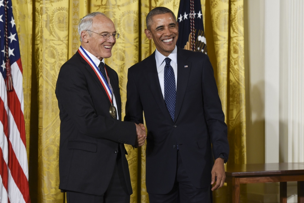
“It was with great sadness that I received the news of Art's passing," said UCSB Chancellor Henry Yang. "A beloved and respected colleague and professor — and a research giant — he inspired all of us who had the privilege of working with him and learning from him. On our campus and around the world, he is held in the highest esteem for his many contributions to condensed-matter physics research and education, including his profound influence on the direction of semiconductor science and technology. I remember how immensely proud we were when he was honored for his pioneering achievements with the prestigious National Medal of Technology and Innovation, presented by President Obama. His impact at UC Santa Barbara and on the international science community will never be forgotten, and more personally, a person of such brilliance and integrity will forever be missed.”
“Art was a true scientific pioneer whose deep understanding of materials science and physics resulted in new groundbreaking heterostructured semiconducting materials as well as new device applications, said Tresa Pollock, interim dean of the UCSB College of Engineering. “Through his research at UCSB, he taught us the true value of collaboration in a collegial environment, and his legacy will long endure.”
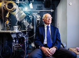
Gossard was a pioneering scientist in materials that would enable the revolution in electronics and photonics. Working closely with UCSB professor and eventual Nobel Laureate Herb Kroemer, Gossard spearheaded the use of a then-novel technique — molecular beam epitaxy (MBE) — a method of “growing” a thin film of one material on top of another by depositing each layer, atom by atom, in an ordered fashion. Gossard, who developed his MBE expertise at Bell labs, had the goal of discovering new physical phenomena and developing high-performance electrical and optical devices. That research would eventually enable dozens of indispensable technologies, including wireless communications equipment, fiber-optics, light-emitting diodes, solar cells cell phones, communication satellites, laptop computers and data centers, optoelectronics, and solid-state lighting.
World-leading materials scientists in the UCSB College of Engineering were quick to recall the historic impact of Gossard’s decades of cutting-edge research.
“Professor Art Gossard was a pioneer in GaAs (gallium arsenide)–based materials and quantum devices,” said UCSB materials professor and Nobel Laureate Shuji Nakamura. “He helped build UCSB into a world-leader in compound semiconductors.”
“Art Gossard was a giant in condensed-matter physics and semiconductor science,” said UCSB materials professor Chris Van de Walle. “He was one of the key scientists who joined UCSB from Bell Labs, and he infused the Materials Department with the spirit of discovery and technological impact that quickly put the department on the map, nationwide and worldwide. I will sorely miss his insights and wisdom.”
“Art was a relatively quiet person, but he was brilliant, extremely bright, and he had a very open mind,” said UCSB emeritus professor of materials and chemistry Galan Stucky. “He was able to see the big picture, and he came up with breakthrough concepts but also could see what you could do with it. Art understood all of that from the basic quantum physics side and all the way through application. He could put all of those things together in a beautiful way.”
“Art Gossard was a world-leading scientist in compound semiconductors and a great mentor to me when I arrived as an assistant professor at UCSB,” said materials professor Steven DenBaars, who co-directs the UCSB Solid State Lighting and Electronics Energy Center (SLEEC) with Nakamura. “His work in quantum materials and devices helped establish our campus as the leading academic center for advanced photonic and electronic devices we all use today.”
Born June 18, 1935 in Ottawa, Illinois, Gossard received his BA in physics from Harvard University in 1956 and a PhD in physics from UC Berkeley in 1960. In his doctoral research, he observed the first nuclear magnetic resonance in a ferromagnetic material and discovered the enhancement of a radio-frequency magnetic field at the nucleus caused by domain rotation and domain wall motion. He then went to work at Bell Labs, where he became a senior member of the technical staff during his service, which lasted from 1960 to 1987. His research there involved molecular beam epitaxy, the growth of quantum wells, nanostructures and superlattices and their applications to high-performance electrical and optical devices and the physics of low-dimensional structures. He created the first alternate monolayer superlattices and the first selectively doped high-mobility heterostructures, and he was a co-discoverer of the Nobel Prize–winning fractional quantum Hall effect. He was also co-discoverer of the quantum-confined Stark effect and optical modulator.
Gossard left Bell labs to join the UCSB faculty in 1987 as a professor with appointments in both the Materials and the Electrical and Computer Engineering Departments. There, he pioneered the growth of epitaxial composites of metallic erbium arsenide and related rare-earth compound nanoparticles in semiconductor hosts. He developed improved thermoelectric materials for the direct creation of electrical power from waste heat and produced semiconductor devices that increased electron-hole tunneling for creation of multicolor solar cells. His work most recently produced high-performance quantum-dot lasers grown epitaxially on on-axis silicon substrates, an advancement that is enabling the replacement of copper with light beams as the interconnects on computer chips.
Over his career, Gossard wrote more than thirteen hundred research papers and received numerous awards including the 1983 Oliver Buckley Condensed Matter Physics prize and the 2001 James McGroddy New Materials prize from the American Physical Society. He was elected to the National Academy of Engineering in 1987 and to the National Academy of Sciences in 2001. He received the U.S. National Medal of Technology and Innovation in 2016.
An article in the Spring 2017 issue of the COE’s Convergence magazine, written by UCSB Public Affairs reporter Sonia Fernandez, recalled some of the early days when Gossard, Kroemer, and their colleagues were pursuing technologies that would not only change the world, but make the digital age and the era of modern wireless electronics possible.
“Being able to put one crystal layer onto another gave you what you needed to make improved transistors and lasers,” said Gossard, who had come to Bell Labs just after receiving his PhD in physics from UC Berkeley in 1960. A specialist in solid-state physics, his interests led him to investigate such phenomena as nuclear magnetic resonance (NMR) in ferromagnets and applying NMR spectroscopy and other advanced techniques to make measurements of new materials.
“I thought the materials themselves were actually more interesting and important than making measurements on them,” he said, so he began focusing on MBE, and Bell Labs responded by pairing him with “genius machinist/super-technician” Bill Wiegmann to work with the earliest versions of MBE machines.
“You couldn’t buy an MBE system back then,” said Gossard. The equipment had to be made in-house and required special attention.
Soon, Gossard and his team were turning out new materials and measuring interesting electron behaviors. Other scientists were turning to them with their ideas for materials and benefiting from Gossard’s solid-state physics expertise and Wiegmann’s technical acumen. They could fabricate increasingly sophisticated materials with, for instance, quantum wells having graded sides to control the behavior and movement of charge carriers, referred to as “doping” a material by adding strategically placed atoms to provide electrons precisely where they were needed.
“We worked more on tailoring the structure than on the chemical composition,” Gossard explained. “You could build a quantum well of any shape, but purity and smoothness of the material were of utmost importance. “Back in California, Kroemer was realizing the potential for using MBE to fabricate semiconductors from different materials having high crystalline qualities, provided the two materials had the same lattice constants, or dimensions of unit cells.
“I decided that molecular beam epitaxy is something that even a theorist can understand,” Kroemer quipped. His job included helping to amplify and steer research efforts at UCSB’s solid-state laboratory, which was part of the university’s emerging College of Engineering.
Instead of jumping into what had already become the highly competitive field of silicon semiconductor technology, Kroemer had convinced Ed Stear, then-chair of the Electrical and Computer Engineering department, to focus on compound semiconductors, which were already showing promise. As part of the effort, Kroemer had managed to acquire an MBE machine, the second one to go to a university.
“He was able to buy one, which was amazing, because he was a theorist and not an experimentalist,” said Gossard, explaining that in the late 1970s and ’80s, MBE was still a relatively new technology. “But on the other hand, he was a very determined visionary, and he saw the opportunity.”
Gossard visited UCSB in 1979 during the second-ever MBE conference in the United States. The gathering, organized by Kroemer, hosted the small but growing community of scientists and engineers interested in the technology and its applications.
Kroemer had his eye on the MBE expert.
“I always said we needed someone like Art Gossard,” he recalled. “I was a great admirer of his work, and he was known to be a fabulous collaborator.”
Gossard actively contributed to UC Santa Barbara throughout his career. He served as Associate Vice Chancellor for Academic Personnel from 2006 until he retired in 2010. He was an avid and competitive sailor and bicyclist throughout his life and commuted to campus on a bicycle or e-bicycle for much of his time at UCSB, into his 80s.
“Coming from Bell labs, Art brought this deep, deep scientific foundation, which was always entwined with technology,” said chemical engineering professor Brad Chmelka. “He was right at the center of that. He was also this very gentle man who was so supportive of young faculty and provided tremendous service, including as associate vice chancellor for academic personnel. That is really giving back. He was inspiring on many, many different levels.”
“Art had tremendous impact on the development of semiconductor heterostructures that are now part of electronics in everyday life, such as cell phones and lasers used in the fiber network critical to the internet,” said UCSB materials professor Chris Palmstrom. “He also had an amazing impact on students, serving on over eighty-five PhD committees. He was a real gentleman, a kind and generous person, and an inspiration for many generations of students.”